pheloniusfriar: (Default)
And finally... a question that did not receive an answer. I'm thinking there might be a way of doing this, but I would need to hear from someone who knows the innards of the PSoC Creator Integrated Development Environment (IDE) on how unless I stumble on some poorly documented back door way of doing it. It maybe impossible from within the component itself though; but it's theoretically possible, and I would view this as a shortcoming of the tool if it's not. Sadly, the tools at Cypress started to balkanize even before they were bought out by Infineon and I'm not getting strong "we'll be supporting these tools going forward" vibes. I'm not plugged in, but it has been over 2 years since the last PSoC Creator update. Not looking good.

Why do I want to do this? If I could get this to work, I could package a UDB-based PSoC component for PSoC Creator to do 16-bit arithmetic with a single 8-bit UDB. I'm a fan of pushing technologies as far as they'll go, so this was a little side project I was working on that was part of a larger project.

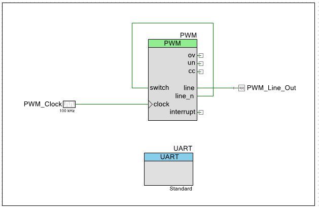
I have a UDB component (single UDB) and was wondering how to initialize the associated Auxiliary Control Register from within the component itself without having to do it at the project level with a call to an initialization API function in main() or some other project-level technique? I want to configure the FIFOs of a UDB into their "Single Buffer" mode by writing 0x03 into the Auxiliary Control Register of that UDB (Architecture TRM, section 16.2.3.7), but can't figure out a way of doing that automatically.

Edit 2020/09/16: To clarify, I am trying to initialize that register at the component level, rather than at the project level, so that someone using the component just has to drag it onto their schematic from the component library, and all the necessary hardware configuration would be done transparently by the component itself simply because it has been instantiated (and not require an initialization function to be called in main() or for the startup code to be modified at the project level). This is the case already for everything but that Auxiliary Control Register. The notion was to make the component potentially a pure "hardware" component from the perspective of someone using it in their project from the component library (it has some parameters that can be set from the schematic, and i was hoping that was all that would needed to be done by someone using it).

I saw in the Component Author Guide the ".cy_registers()" function (section 4.3.5 "Fixed Blocks") that "For all fixed blocks, a parameter of cy_registers is available to allow you to explicitly set the values for the given registers for the block. The values listed will be included in the configuration bitstream generated to program the part, which will be established before the main() function is called." This seems to be exactly what I want, but it doesn't seem that the datapath itself allows this parameter. When I look at the .vh2 file created for the component, the instance of cy_clock_v1_0 that I put on my schematic (and wired to my component) has a parameter "cy_registers" (it's empty, but it's listed); but the cy_psoc3_dp I instantiated does not have such a parameter listed. When I tried to add it to the parameter list of the datapath, I get an error.

Is there a "proper" way of doing this from within my component so the value is automagically intialized by the time main() runs? I wanted the component to be able to run without needing to be initialized in the user's software (effectively a pre-configured hardware component), and the FIFO configuration is the only thing I can't seem to access from within my Verilog code (and it won't work without the FIFOs being in the proper mode). I hope I'm just missing something obvious.

I'm guessing that the cyfitter_cfg() function can do it (and is where this should end up), but I can't figure out how to get it in there (there's a BS_UDB_0_0_0_CONFIG_VAL[] array in the cyfitter_cfg.c file that was created that seems to have the UDB config in it, and presumably the Auxiliary Control Register is one of those values). I read through Alan Hawse's excellent IoTExpert article on PSoC startup, and it told me where it would be done, but provided me with no clues on how to get it done.

PSoC4 Boot Sequence (Part 5) – Initializing the PSoC with initialize_psoc()


[I'm thinking I should probably save that Blog before it gets deleted some day as well... it's irreplaceable information]

A user [RodolfoGL] tried to help, and posted:

I don't think it will make any difference setting the FIFOs during startup or in the main(). In any case, if you want to customize the startup code, you need to import the cy_boot component. See how to do here:

PSoC Creator Tutorial - Importing and Copying Components - YouTube

Then open the PSoC4/API/Cm0Start.c to do your changes.


I wrote back:

Thanks for the suggestion. I watched the video and thought about it, and that isn't what I want to do. When I was asking my question, I wasn't entirely sure I was being clear, and I was not (I will edit my question to clarify). As you say, doing it this way, or having an initialization function that gets called by the user in main() makes no difference because it is happening at the project level. What I realized I should have said was that I am trying to initialize that register at the component level, so that someone using the component just has to drag it onto their schematic, and all the necessary hardware configuration is done transparently by the component itself (and not require an initialization function to be called in main() or for the startup code to be modified... although it's good to know that technique for my own projects now that you've pointed it out to me). This is the case for everything but that Auxiliary Control Register. The notion was to make the component potentially a pure "hardware" component from the perspective of someone using it in their project from the component library (it has some parameters that can be set from the schematic, and i was hoping that was all that needed to be done by someone using it). Thanks for helping me refine my question.

To which they replied (kind of confirming where I was stuck):

I understand now what you want. I'm not aware a way to do this automatically. I think the only way is to create an API for your component and let the user call it in the main().

So, I wrote again, hoping someone else might jump on when they realized what I was looking for (no takers):

That is what I'm suspecting as well, but am hoping I've missed something.

I am wondering now, looking at the wording, whether there's a back door I can use? Section 4.3.5 "Fixed Blocks" in the Component Author Guide, it says "For all fixed blocks, a parameter of cy_registers is available". In referring to the figure in section 4.3.1.1 "UDB Overview" it says "The blocks are color coded to differentiate between the types. Purple is a register, blue is a fixed block that performs a defined function, ...". The only blue block ("fixed block") that I can instantiate explicitly in my code is the cy_psoc3_count7 block, so I wonder if it will accept a cy_registers parameter? And if it does, will it check what register directive I pass in to it? The cy_registers parameter is not listed in the instantiation list in the guide for cy_psoc3_count7, so I am guessing this will not work, but I'll give it a try Wednesday (hopefully) and report back.

I scoured the Internet before I asked my question and have not been able to find a single reference to cy_registers, so I am not even sure how (or if) it is supposed to be used. The fact that it was listed in the "Implement a UDB Component" section suggests that there should be some way to access this capability from a library component's Verilog code. But maybe that's not the case, I don't know.


So I tried, and failed:

In a surprise to nobody, and despite the glimmer of hope from the wording in the Component Author Guide, the cy_psoc3_count7 component does not accept cy_registers as an argument.

This compiles fine:

cy_psoc3_count7 #(.cy_period(7'b1111111))

    C7Counter (.clock(CLK), .reset(1'b0), .load(1'b0), .enable(1'b1), .count(), .tc());

This results in the error, "'cy_registers' not a parameter of module 'cy_psoc3_count7'" during synthesis:

cy_psoc3_count7 #(.cy_period(7'b1111111), .cy_registers(""))

    C7Counter (.clock(CLK), .reset(1'b0), .load(1'b0), .enable(1'b1), .count(), .tc());

I guess unless someone from Cypress can help, I'll need to re-think my plans on this.


I kind of put the project aside because I couldn't get an answer, but hope to dust it off some day since it's a neat idea if I can make it work.

And last, but not least, Season 1, Episode 20:

pheloniusfriar: (Default)
The penultimate PSoC technical post "port" from the community forums to here for my own use. I'm kind of proud of this one because it's a really deep dive into technologies that are a little bit "black box" and this was some intense exploration on my part. If anyone else has done this, they certainly hadn't published anything.

I wanted to do this, but could not find any reference (one way or the other) to being able to use the Parallel Input (PI) to the datapath as a constant for calculations with the ALU (e.g. add or subtract), so I decided to give it a try because this would be very helpful in one of the things I'm trying to do with UDBs.

The answer? Yes, you can use the PI as a constant! I have attached a simple project to demonstrate this (I did it on a CY8CKIT-049-42xx, you'll need to reconfigure the Bootloadable component with your elf/hex files for it if you try to compile it for the same target).

Since there's not a lot of documentation on using the PI, much less in this manner (I really couldn't find anything that mentioned using PI as a constant, but my search skills may not be 100%), I thought I should document what I did and share it with others. Following the general steps outlined in AN82156 "Designing PSoC Creator Components with UDB Datapaths", section A.5 "Project #5 – Parallel In and Parallel Out", I created a component symbol, added a parameter called "PI_Value" that I set to 5 as default, and created a blank Verilog file for it. The parameter constant was added automatically when the Verilog file was created from the symbol editor, fyi. I then used the Datapath Configuration Tool per the instructions in AN82156 and created a blank cy_psoc3_dp datapath instance in the Verilog file. In the tool, first enabled the PI_DYN bit, then set it to EN. I created two datapath instructions: one to add the value of PI to the value of A1 and then store it back in A1 (FUNC = ADD, SRCA = A1, SRCB = A1, A1_WR_SRC = ALU, and CFB_EN = ENBL... the last of which dynamically selects PI as the input for SRCA to the ALU rather than A0 or A1 when the static PI_DYN bit is EN), and the other to just pass the value of A1 through the ALU (with FUNC = PASS, SRCA = A1, SRCB = A1, CFB_EN = DSBL). My Verilog then just flips between the two states every clock. The idea was that the first state would add 5 to A1 every time it ran, and that's what it does (the second state does nothing, but I wanted to have something heading into different states to make it a bit more representative). To finish up the datapath configuration in the Verilog file, I made the following assignments: .clk(Clock), .cs_addr( { 1'b0, 1'b0, next_state } ), .pi(PI_Value), and .po(po), where next_state was a simple flip-flop "reg next_state;"). So .pi() was passed the constant I had defined at the component level. There's a bit of wiring around the Parallel Output (PO) because I have a little LED board I made so I could watch the state transitions on port P2[7:0] (and that's why the frequency is so slow as well... so I could easily count the binary to make sure it was increment by 5). Note, writing ".po({Out7,Out6,Out5,Out4,Out3,Out2,Out1,Out0});" also seemed to synthesize fine and saved that extra wiring and assign statements (I didn't test it out on hardware though). I was trying to emulate the style of AN82156.

So, there were two things I wanted to mention before wrapping up. The first is that the way PO works is not immediately clear from the basic datapath diagram that appears in a lot of the documentation (e.g. the TRM, Rev *H, Figure 16-6 "Datapath Top-Level"). The implication is that PI, A0, and A1 are multiplexed onto SRCA to the ALU, and that PO is connected to the SRCA connection itself (this is literally how it's drawn in that figure). That was one of the reasons why I initially made two different datapath states: because I thought that in the ADD state, since I was routing PI to SRCA, that I would see it on PO. I added the second state so A1 would be applied to SRCA and PO would then alternate between PI and A1 (I needed to see A1, but seeing the constant every second cycle was fine). It didn't work that way... all I got out of PO was the value for A1. I had to dig deep into the TRM to find the answer, but in section 16.2.2.8 of the TRM (Rev. *H) "Datapath Parallel Inputs and Outputs", there is another diagram (Figure 16-25 "Datapath Parallel In/Out") that shows the insides of the SRCA multiplexer. In this diagram, it is shown that there are two multiplexers: one that selects between A0 and A1 that feeds into a second multiplexer whose other input is PI. PO is connected to the output of the first multiplexer... so that PO can never see the value of PI, and even when PI is being used, PO will be connecting to either A0 or A1 only. Mystery solved. But ugh.

Lastly, there seems to be a couple of bugs in AN82156 "Designing PSoC Creator Components with UDB Datapaths", section A.5 "Project #5 – Parallel In and Parallel Out". It assigns two bits to a one bit register ("state"), and then suggest a non-blocking assigning of the PO value out of the datapath to the component's output:

// From AN82156 ... bugs?
reg state;
wire[7:0] po;

localparam STATE_LOAD = 2'b00;
localparam STATE_ADD = 2'b01;

always @( posedge clk )
begin
  case (state)
    STATE_LOAD:
      begin
        state <= STATE_ADD;
        /* we must latch the PO value here, because in the next state PO is not valid*/
        Parallel_Out <= po;
      end
  STATE_ADD:
    begin
      state <= STATE_LOAD;
    end
  endcase
end

But Warp would complain (rightfully so I think) when I tried it with my component, that Out7 through Out0 were "not a register type", and could not be assigned in that way. I may be doing something wrong (let me know if you know what it is), since I am no expert at this.

// *** Does not work!!! ***
wire [7:0] po;
reg next_state;

always @ (posedge Clock)
begin
  case(next_state)
    1'b0:
      begin
        Out7 <= po[7]; Out6 <= po[6]; Out5 <= po[5]; Out4 <= po[4];
        Out3 <= po[3]; Out2 <= po[2]; Out1 <= po[1]; Out0 <= po[0];
        next_state <= 1'b1;
      end
    1'b1:
      begin
        next_state <= 1'b0;
      end
  endcase
end

In my case at least, fIguring out how to use UDBs is hard enough without these couple of additional issues.

One last thought (I haven't tried this yet, it's next on my list). Since the the SUB function of the ALU is "SRCA - SRCB", if A1 is SRCB, it is not possible to subtract PI from it (and store it back in A1, for instance). However, if PI is stored as an 8-bit 2's complement negative number and is added to the A1 register instead of subtracted, then the result will be that the PI value is effectively subtracted from the A1 value. I need to figure out the flags, but this seems like it should work fine. Again, I haven't tried it, but maybe setting the parameter as an int8 instead of a uint8 will allow negative numbers and will encode it properly.

Edit 2020/09/10: I did try what I suggested with the 2's complement arithmetic and it worked like a charm. For instance, to subtract 5 by using the ADD function of the ALU, I set PI to -5 in 2's complement (".pi(8'b11111011)") in the datapath setup, and tried ADDing it with a few values like 10, 5, and 3, and I got the correct answers (which was expected). I wanted to know what the flags were set to so I could figure out the best way to do 16-bit arithmetic on a single 8-bit datapath, so I used A1 as the MSB and A0 as the LSB. What is extra nice, is the state of the carry out bit is 0 if the "addition" of the 2's complement PI to A0 results in a negative number, and 1 if not. I used the registered carry flag input to a DEC command on the MSB register (A1), and it performed the operation A1 <- A1 - 1 + carry (carry is 1 if ADD PI + A0 is a positive number, so the DEC A1 command with the registered carry option gives A1 <- A1 - 1 + 1, so A1 doesn't get decremented; but if PI > A0 and the operation ends up with a negative result, the operation is A1 <- A1 - 1 + 0, which decrements A1). So this can be used for 16-bit arithmetic on the 8-bit ALU with two cycles! I double-checked the SUB command on the ALU, subtracting A0 <- A0 - A1 for instance, and the carry flag (which the spec says is "inverted" for SUB results, but I wasn't sure what that meant exactly), let's you use the DEC A1 command with registered carry again to do proper 16-bit math. Just fyi.

Edit 2020/09/14: Short summary: this technique uses a macrocell! Long summary: I was working on my component that used the above technique and I kept seeing an extra macrocell being used. I had declared 4 registers, but 5 macrocells were being allocated to the design and it was driving me nuts trying to figure out what was causing it. I had assumed I had messed up an if or case statement or something and was causing an implicit latch instantiation, but nothing I did seemed to make any difference (and from what I can tell, Warp doesn't care if you're missing a final else statement, or if you haven't specified all possible cases in a case statement... it doesn't create implicit latches like other synthesizers in those cases it seems). I eventually broke down and started rummaging in the PSoC Creator file output and got my answer. It turns out the extra macrocell was used to provide the value to the Parallel Input (which is why I mention it here). In the "codegentemp" there was a file _p.vh2 that is the VHDL translation of the Verilog code it looks like. In it, there was a macrocell definition called "__ONE__". The only thing this macrocell does is supply logic 1s to the appropriate bits in the value provided to the Parallel Input. If I set .pi(0) in the datapath instantiation, the macrocell goes away. I had thought that the constant bits would be supplied through a connection with the routing channels (like there was a magic source of 1s and 0s available on it), but it seems that a macrocell in the UDB is needed to supply that logic level. Fair enough, but it's good to know that one of the macrocells will be used if you use the Parallel Input to supply a constant value. I have enough to spare, but was worried it was something more potentially vexing. I don't know where the 0s are coming from (the PI bits that were logic 0 were not connected in the netlist to anything), but I'm not too concerned, it works fine. In the code below, it was set as ".pi(8'b11111011)".

\TEST_COMP:DP_INST\:datapathcell
        GENERIC MAP(
            [ ... bunch of config deleted ...]
            uses_p_out => '0',
            clk_inv => '0',
            clken_mode => 1)
        PORT MAP(
            clock => Net_35_digital,
            cs_addr_2 => \TEST_COMP:state_2\,
            cs_addr_1 => \TEST_COMP:state_1\,
            cs_addr_0 => \TEST_COMP:state_0\,
            ce0_comb => \TEST_COMP:lsb_equal\,
            z0_comb => \TEST_COMP:lsb_zero\,
            ce1_comb => \TEST_COMP:msb_equal\,
            z1_comb => \TEST_COMP:msb_zero\,
            p_in_7 => __ONE__,
            p_in_6 => __ONE__,
            p_in_5 => __ONE__,
            p_in_4 => __ONE__,
            p_in_3 => __ONE__,
            p_in_1 => __ONE__,
            p_in_0 => __ONE__,
            busclk => ClockBlock_HFClk);
    __ONE__:macrocell
        GENERIC MAP(
            eqn_main => "1'b0",
            regmode => 0,
            clken_mode => 1)
        PORT MAP(
            q => __ONE__);

I am getting closer to being done now that this is resolved as well.


And the only response was a thank you from a mod for sharing the info with the community (which is cool, don't get me wrong).

And now, on with the show: Season 1, Episode 21:

pheloniusfriar: (Default)
Now comes the crux of this (temporary... two more to go) series of "porting" my posts from PSoC user forums to here: I had a question, got community help, and the final answer is absolutely beautiful and elegant. As I stated at the end of the thread to the person who provided the solution: "I used a sledgehammer to solve the problem, and once the requirements were clear, you used a feather". I really flailed with this because I failed to understand a key concept on how the TCPWM component worked. I was working with this component again recently and I thought of this exchange, and it motivated me to check to see if it was still there, and that fear of Dark Ages information loss prompted me to put in the effort to copy over all of my posts from there.

I have been trying to get a glitchless PWM working on a PSoC 4200 (I had in the past and was dusting off the old project), and I cannot seem to get the PWM Swap to work no matter what I try. I have attached a project that instantiates a PWM. I have the Line output connected to an LED so I can see the output of the PWM (it's on a CY8CKIT-049-42xx, so port 1.6), and am driving the PWM clock with a 1Hz clock so I can easily time the LED changing. In the configuration for the PWM component in PSoC Creator 4.3, I set the Period to 9 (I want a period of 10 seconds, and the datasheet says to set it to N - 1... that seems to work fine). I set the Compare Register to 2, I set the Compare Register Buffer to 6, and I turn on the Swap flag. The PWM is set to left align mode as well, and have turned off the interrupt. I'm keeping it simple with my example. The code in main does two things (my component is named PWM): "PWM_Start(); for(;;) CySysPmSleep();" ... so start the PWM component and put the processor to sleep. This is the simplest configuration I could come up with and it still doesn't work for me.

I program it into the 4200 and ... the LED stays on for 2 seconds, stays off for 8 seconds, stays on for 2 seconds, stays off for 8... etc. The Compare Register Buffer value never gets swapped with the Compare Register at TC per the documentation. I have tried a very large number of things including using the software to also set the swap flag to on ("PWM_SetCompareSwap(1);"), I've checked that the "ov" output is pulsing every 10 seconds (yup). In the component configuration, I have changed the Compare Register value to 4 and the Compare Register Buffer value to 8 just to make sure I'm programming the chip, and ... on for 4 seconds, off for 6 seconds, etc... never swapping in the buffered value. I've looked at all the documentation I could find. I've tried turning on the "switch" input and connecting it to the "ov" output (with a falling edge trigger). Nothing has worked. I set up an interrupt handler (not in the attached example) and verified that it was being called at TC... yup... I could write a value into Compare Register Buffer from the interrupt handler and ... it never gets swapped into the Compare Register, so no matter what I write, the PWM only reacts to the initial value of the Compare Register.

I have a running application on an identical PSoC 4200 that uses this technique, but compiled it with a much older version of PSoC Creator (probably something in the 3.x timeframe) and I just duplicated the code over for this project, and it definitely does not work anymore. Has something in PSoC Creator broken, has the component implementation in PSoC Creator changed, am I missing something very simple? I know it's not the hardware having changed, because it's the the same chips that used to work. What is particularly galling is that in the PWM component configuration window, it actually shows the expected waveform from the Line output, and it shows it high for 2 clocks, and then low for 8, then high for 6 clocks, and then low for 4. That does hint that something has gone wrong somewhere. I'm stumped. Any thoughts?


I got a response from a member of the community [MotooTanaka] on what they ended up doing to try to get it to work. It was WAY more effort than I could have possibly expected, and even then wasn't the direction I wanted to move toward (it required software, and I wanted a purely hardware solution if possible). Note: It's interesting in that it uses the serial port out to the PC as a status output, which is a good thing to remember that I can do when debugging (I forget sometimes).

Yes, this was(is) a very tough one. Just like you I tried for a few hours with series of failures... And in the datasheet of TCPWM, I found the following description:

void TCPWM_SetCompareSwap(uint32 swapEnable)

Description:
Writes the register that controls whether the compare registers are swapped. When enabled in Timer/Counter mode (without capture) the swap occurs at a compare/capture event. In PWM mode the swap occurs at the next TC event following a hardware switch event. Not applicable for Timer/Counter with Capture or in Quadrature Decoder modes.

Parameters:
uint32 swapEnable: 0 = Disable swap; 1 = Enable swap.


This sounds like we need a "switch" event before the "TC" event. So I made the following project, using CY8CKIT-042. Note: Actually the following is the only project I could make the swap work. And in the ISR I needed to put CyDelay(2) to generate a long enough pulse width from the Control_Reg. Probably it could be done in the main loop. After that I tried a several hardware approaches but in vain. So my current conclusion is that we seem to need provide "switch" event before TC event, and it must have enough pulse width for PWM to detect (or set something inside).

Schematic, pinouts, source code, and log output behind cut )


Again, I wanted a purely hardware solution, but... this laid the foundation for the solution. I wrote back:

I am overwhelmed by how much work you put into this. Thank you so much!

My frustration was that I definitely had it working, and it definitely was not working in this case. The documentation is quite contradictory, but your statement that a "switch" event is required matches my previous experience (and probably some random note I found somewhere when I was doing my earlier design). Your investigation and success doing it with an interrupt routine in software, led me to figure it out. Your statement that "I needed to put CyDelay(2) to generate a long enough pulse width" was what allowed me to find the relevant pieces of documentation that explained the situation.

The first piece of relevant information is at the bottom of the "Outputs" section of the TCPWM datasheet: "The overflow (ov), underflow (un), and compare/capture (cc) output signals have two HFCLK cycle pulse width for PSoC 4100/PSoC 4200 devices". So the "ov" output pulse is only two HFCLK clock cycles wide. The other needed piece of information is at the bottom of the "Inputs" section: "All inputs are double synchronized in the TCPWM. The synchronizer is run at HFCLK speed. After that (just for PSoC 4000, PSoC 4100, PSoC 4200, (Timer/Counter, PWM modes)), these signals are synchronized with the component clock." So... the "switch" input is sampled on the rising edge of the PWM "clock" signal, which in my case for this test is 1Hz. Since the "ov" is such a short pulse, it is long, long gone before it can be sampled by the 1Hz input clock if the "ov" signal is just looped back to the "switch" signal (which is what my original design that worked did). I should further mention to anyone reading this that the description of the Compare Swap feature in the datasheet is wrong. It currently says, "the swap selection causes the two compare values to swap at each TC event"; but it should say "the swap selection causes the two compare values to swap at each TC event if a switch event has occurred".


Then there's the question of why my earlier design did work. The answer to that makes sense now as well: I was clocking the PWM at HFCLK (48MHz in my case), so in looping the "ov" signal back to "switch" worked fine at triggering a switch event. The "ov" pulse is two HFCLK clock cycles long, and I had the "switch" configuration parameter set to trigger on a falling edge pulse, so the "switch" input would properly sample the high pulse because it was high long enough to be latched by the HFCLK clock signal, and then would properly sample the "ov" output going low again, and would trigger a switch event for the next TC. It would work as well if I had it set to switch on a low to rising edge. It seems I was just lucky with my earlier design because I didn't realize the "ov" signal issue -- I assumed it was clocked out with the PWM clock and would be high for one full PWM clock cycle (I was wrong on the number of clock cycles too since it is high for two HFCLK cycles) as this makes more sense to me as it allows for a full and easy hardware implementation of the register swapping at lower PWM clock frequencies. I think Cypress designers made a bit of a mistake with this decision to use an HFCLK-based pulse rather than a signal clocked with the PWM "clock" signal. Oh well, they're not going to be able to change it now as this is a hardware component and it can be made to work.

I really do want to do my design in hardware, so I figured out a way of using the on-chip programmable logic to allow the "ov" output to generate a signal usable by the "switch" input circuitry. This is an all-hardware solution as well. The Period has to be set to at least 2 (N - 1), so the PWM counts for at least 3 PWM clock cycles. The switch input is set to be a rising edge triggered event.The software is the same (turn on the PWM component and put the processor to sleep). Project attached.


There is definitely a chance for metastability issues since we don't know precisely what the phase relationship is between the HFCLK and the PWM "clock". To that end, I invert the "ov" signal before clocking the first flip-flop with it. This guarantees at least two HFCLK cycles between when the PWM clock goes high (to trigger the "ov" signal) and when the "ov" signal goes low again at the end of the pulse. Depending on how the "ov" pulse is generated, it could be three or more HFCLK cycles before the falling edge (since it is a signal potentially going between clock domains, they probably have a synchronizer on it). As long as half the cycle time of the PWM clock is longer than the maximum time between the rising edge of the PWM clock and the falling edge of "ov" (plus the time needed for the signal to propagate through the first flip-flop to its Q output and the setup time needed for the second flip flop before it is clocked by the low-going edge of the PWM clock), then there will be no metastability problems. Because I'm not sure what the worst case is for when the "ov" pulse happens after the PWM clock triggers the signal (by causing the count to roll over from TC to 0), I can't make a guess at what the maximum safe frequency would be for this circuit. I'm sure it's fine into the MHz region, but I can't know for sure.

Here's the timing diagram for the above circuit:


Depending on the PWM clock frequency you need, if it's high enough and there's a worry about metastability, just clock the PWM at HFCLK and use the prescaler setting to bring the frequency down to where you need it. Since the prescaler can go from 1 to 128 (in powers of 2), use HFCLK/128 as the upper limit of where you might need to use this circuit. So for a 48MHz HFCLK, upper limit would be 375kHz (and for anything below that you probably need to use this circuit to get the switch swap to work). I have attached my modified circuit. Note that the project generates two warnings because PSoC Creator 4.3 recognizes that the circuit goes between clock domains without proper synchronization. As described above, the timing is okay as long as the PWM cycle time is sufficiently long compared to when the falling edge of "ov" occurs.

With these high and low speed techniques available for doing the Compare Register swapping, it can be done with any PWM clock frequency. Either allows for the glitchless operation of the PWM where the Compare Register Buffer can be updated in an interrupt handler triggered by the PWM TC event. The Buffered value is then automatically and cleanly swapped into the Compare Register at the TC event because a switch event happened in the last cycle. As long as the interrupt handler can run before the TC (in my earlier project, I used a Period count of 2177 at 48MHz, and woke the CPU up from a CySysPmSleep to process the interrupt, and there was plenty of time). The code I used in my old project to do this was as follows. I, of course, turned on the Interrupt on Terminal Count option on the PWM component and attached an Interrupt component (called "PWM_TC_ISR" in the code here).

CY_ISR(PWM_Next_Value) {
    PWM_WriteCompareBuf(<>);
    PWM_ClearInterrupt(PWM_INTR_MASK_TC); }

int main() {
    PWM_TC_ISR_StartEx(PWM_Next_Value); PWM_Init();

    // Write the first two samples into the PWM
    PWM_WriteCompare(<>);
    PWM_WriteCompareBuf(<>);

    CyGlobalIntEnable; PWM_Enable();  // Only starts it, does not re-initialize
    for(;;) { CySysPmSleep(); } }

Thank you again very much for your help!


To which the community member goes S-Tier and answers:

Thank you very much for your throughout explanation! Finally I understood with what we were fighting yesterday. BTW, reading your "paper", following (a kind of) stupid Idea came to my mind. At first I thought that I'd use a counter to generate the switch event. But we need to avoid immediate after the TC, and the width must be 2 or greater. Seeing the PWM configure dialog,


I thought... didn't we have a "counter" here? So if, and only IF, you can keep the compare between 2 to period-2, line_n seems to work for the purpose. So I modified the schematic as:


And... it works!


As I wrote above this trick works only 2 ~ period-2, but if your application put up with this limitation, this is quite an easy trick. Last but not least, I agree with you that the description in the datasheet was not kind nor sufficient for usual people like us.


Mind. Blown. So simple, so beautiful!

Hahahaha, I used a sledgehammer to solve the problem, and once the requirements were clear, you used a feather! That is definitely the optimal solution for the Compare register swap problem in almost all cases (provided, as you say, one can live within the compare value limitations), and it requires no additional system resources.

If you use a "Falling edge" trigger instead on the "switch" input, there is no limitation on the upper value for the Compare value (it can equal Period). Also, because the Period is actually set to N - 1 of the number of cycles (N) you want to count to [from the Period description for the PWM mode in the datasheet: "to cause the counter to count for N cycles, this register should be written with N-1 (counts from 0 to period inclusive)"], you can also go as low as 1 in the Compare register. I tested this with your loopback configuration and the Falling Edge trigger of "switch" with a Period of 9 (10 clock cycles), with a Compare Register of 1 and a Compare Register Buffer of 9, and it worked fine. I have attached the project.

Thank you again for providing a truly elegant solution to this problem.


And this, my friends, is how community can work together to solve hard to understand problems in elegant ways.

And here's more entertainment... Season 1, Episode 22:

pheloniusfriar: (Default)
Here's the announcement I made for the KiCad PSoC 4200 Family library. Since I control most of the files on my own server, this is just here to preserve the words of the announcement. But... even there, the URLs have changed from Cypress to Infineon for a few of them. To their credit, the Cypress URLs redirect to the Infineon equivalent page (at least as I write this), so I'm impressed. On the other hand, what used to be kicad-pcb dot org is now kicad dot org, and the old domain doesn't redirect. Not impressed. Even the smallest of little pages with hyperlinks to outside sources has experienced link rot in two short years. It's a real problem. I have, of course, fixed the links for this posting. Also, at the end, I include a link to the FreeCAD source file for the WLCSP 3D model I designed for KiCad board visualization.

I needed a KiCad library for the PSoC 4200 Family of MCUs, and I could not find one (Cypress had libraries for Allegro, Altium, and Pads, but not KiCad), so I created one myself. It can be downloaded from this page: PSoC 4200 MCU Family Library for KiCad.

The library contains a complete set of schematic symbols, and all associated footprints and 3D models not included in the standard libraries (the WLCSP package in this case), for doing designs with KiCad using any of the PSoC 4200 Family of MCUs. It includes support for all five packages available: CY8C42xxAXx (44-pin TQFP), CY8C42xxAZx (48-pin TQFP), CY8C42xxFNx (35-ball WLCSP), CY8C42xxLQx (40-pad QFN), and CY8C42xxPVx (28-pin SSOP). The schematic symbols show the pin functionality available for its associated package. Note that the internal configuration between the different models of the PSoC 4200 using the same package are not shown (it’s a generic schematic symbol and associated footprint that will work for all of the variations that use the same package). The secondary port functions that are common across all variants of the part in a particular package are shown. Specifically, the external voltage reference, wake up, external clock, and Serial-Wire Debug (SWD) pin associations are all shown.

The library archive contains a README.TXT file with a description of the library and installation instructions to use it with KiCad. The LICENSE.TXT file contains the license it was released under. Fyi, the license is effectively same as the KiCad Library License: the CC-BY-SA 4.0 license with an exception to allow any works that use the library to be unencumbered by any particular licensing restrictions (again, see the KiCad Library License or the LICENSE.TXT file distributed with the archive).


Here's the FreeCAD source file for the WLCSP 3D model I included in my parts library for KiCad (I did not include this with my announcement post, so I guess this is "bonus content", heh):

PSoC 4200 WLCSP-35 3D Model for KiCad

The STEP and VRML files need to be exported from FreeCAD using this source, here's the "cheat sheet" (it's not a trivial process, fyi, but the tools are available and free):

KiCad StepUp tools cheat sheet (PDF)

The footprint is created in KiCad (the .kicad_mod file, or just .mod in KiCad 6 and later), but then it needs to be aligned with the 3D model. This step is important for the rendering to work properly. The PDF I linked to has links to everything needed and some tutorials on how to do it. Be patient with yourself, the first time through is tricky.

And here's the next show in reverse order (since I started doing it, might as well continue): Season 1, Episode 23 (the Discordian/chaos edition show).

pheloniusfriar: (Default)
And here's the next installment of my "hey I wrote stuff somewhere else, I'll copy it over here too" thing. This post also unexpectedly ended up justifying the fact I'm doing this: companies change, get bought out, and important legacy information can be lost forever. Not that my posts are "important", but an entire blog that existed when I made my initial post is gone... and there is no official backup anywhere. It's concerning, and speaks to what people refer to as "a new Dark Age" that we are living in — where knowledge relied on by previous generations is lost forever as digital assets are thoughtlessly destroyed or become unreadable because of the format they are in. The willful or ignorant deletion of information not quite what is considered as a harbinger of this new Dark Age (which is what is at play here), but I lump it in because it's even more insidious (don't it always seem to go, you don't know what you have 'til it's gone?).

So... I was working on a PSoC 4200 parts library for KiCad (a free, open source, schematic capture and PCB design package, supported by CERN these days), and one of the packages it came in (WLCSP) was not really supported. I was curious, and posted this.

I downloaded the official PSoC 4200 PCB footprint libraries for Allegro, Altium, and Pads and there does not seem to be an official footprint for the WLCSP 35-ball package (the FN package). I have the 4200 family datasheet (001-87197 Rev. *J), and there is a drawing of the package on page 38, but no corresponding footprint specification. I have read JEDEC Design Guide 4.18 per the instructions in the datasheet, but it (as expected) only describes the package, not the recommended PCB footprint. I, of course, have the die WLCSP package size and pad spacing from the datasheet, so that's not an issue. All I need is the recommended pad size to complete the footprint myself. Any suggestions?

Edit: I found an application note from Freescale (now NXP), AN3846: Wafer Level Chip Scale Package (WLCSP), from 2012 that provides guidance for their WLCSP packages for both PCB layout and manufacturing. There is a copy here:

https://www.mouser.com/pdfdocs/AN3846.PDF

They say their their solder balls are 0.250mm in diameter, but Cypress says theirs are 0.260mm. I am going to guess that if I scaled the pad sizes by 0.260mm/0.250mm = 1.04, that I would get the right pad sizes for the process specified by Freescale/NXP. It's a bit of a bummer that Cypress doesn't seem to have any guidance at all on this even though they provide WLCSP packaged chips.


As a bit of background (from the above AN3846 application note):

Wafer Level Chip Scale Package refers to the technology of packaging an integrated circuit at the wafer level, instead of the traditional process of assembling individual units in packages after dicing them from a wafer. This process is an extension of the wafer Fab processes, where the device interconnects and protection are accomplished using the traditional fab processes and tools. In the final form, the device is a die with an array pattern of bumps or solder balls attached at an I/O pitch that is compatible with traditional circuit board assembly processes. WLCSP is a true chip-scale packaging (CSP) technology, since the resulting package is of the same size of the die (Figure 1). WLCSP technology differs from other ball-grid array (BGA) and laminate-based CSPs in that no bond wires or interposer connections are required. The key advantages of the WLCSP is the die to PCB inductance is minimized, reduced package size, and enhanced thermal conduction characteristics.

It's pretty "top shelf" integration and I was curious about exploring their use for various ideas I had. I am also a completionist, so if the PSoC 4200 was available as a WLCSP die, then I wanted it for the library I was putting together.

There were no takers to my question, but I found the answer myself:

Well, I managed to find the Cypress equivalent of the Freescale/NXP document on WLCSP requirements! It was not easy though (I had to follow a bread-crumb trail from older documents that hinted that such a thing existed, even though it ended up having a very different name now). Here it is:

AN69061 - Design, Manufacturing, and Handling Guidelines for Cypress Wafer Level Chip Scale Packages

It has all the information needed to design the PCB. I also found this note from Mentor-Graphics that has a lot of information:

[And this is the "info loss" link I mentioned above... see below]
PCB Design Perfection Starts in the CAD Library – Part 11

And apparently there is a tool called "PCB Libraries" that has an "IPC-7351 Calculator" that will generate the industry standard right sized pads based on your input about the package and layout technique you want to use (NSMD vs. SMD). I haven't tried it myself, but they say there are free versions.

PCB Libraries

Anyway, I think I have my answer sufficient that I can generate my own footprint now and have it agree with industry standards (IPC-7351 apparently... a "pay for play" document unfortunately).


Someone [MotooTanaka] did reply: "Reading your question, I also tried to find one. But with my ability I could not. You've done a great job!". So I was not the only one.

Now... to the problem... One of the most useful resources I ran across addressing the issue of how to design PCBs for these advanced technologies was a blog by Tom Hausherr (from the early 2010s) on the Mentor Graphics website (they designed chip and printed circuit board design software, etc.). Mentor Graphics was bought by the German multinational conglomorate Siemens AG in January 2021 and because Siemens EDA. When my post was written in April 2020, this had not yet happened. Since then... the Hausherr blog appears to have been discarded and is no longer officially accessible. A victim of this New Dark Age of digital information and knowledge and know-how it seems.

So what to do for this post??? Well, I don't want to include broken links because then I'm just rolling my eyes and moving on, and this really useful information just disappears under my watch as well. I spent probably an hour looking for an archive of Hausherr's blog. I found some RSS references (but they just pointed back to the now defunct URL of the original blog), I found a PDF archive of his posts at a design info site... up to Part 10 (I was referencing Part 11). I also found out that he had written 19 parts (the last one was in 2011). Then it occurred to me... The Wayback Machine! I typed in the URL and ... score!!! Here it is:

PCB Design Perfection Starts in the CAD Library – Part 11

The other parts appear to be there too (use "http://blogs.mentor.com/tom-hausherr/" in the Wayback Machine)! And as I was rummaging around trying to finish this post, I found a PDF of Parts 11 through 19 of the blog, yay! There is a good list of the URLs to the 19 parts on the subject here (or at least there was when I wrote this). Here are the PDFs (on the Chinese edatop web site), which will no doubt disappear someday too.

Tom Hausherr "PCB Design Perfection Starts in the CAD Library" Parts 1 through 10 (PDF)
Tom Hausherr "PCB Design Perfection Starts in the CAD Library" Parts 11 through 19 (PDF)

[A little hacker-esque knowledge here... if you go to "http://www.edatop.com/down/faq/pads/", their directory contents were exposed when I wrote this and you can potentially download the thousands of documents and other files there... don't tell them I sent you if you go rummaging]

Anyway, for the KiCad library, see my next post.

And I may as well keep the entertainment going at the end of these posts. Here's Season 1, Episode 24.

pheloniusfriar: (Default)
Copying another post I made on the Cypress/Infineon user forum here so I have it myself.

I have written an article on my blog on the process I followed to get an audio clip into a PSoC 4200 MCU (I used the CY8CKIT-049-42xx PSoC 4 Prototyping Kit), and play it back using a TCPWM component. I start with a 44.1kHz 16-bit PCM stereo audio recording (CD quality), and go step-by-step on how to process the audio, reduce the dynamic range (bits per sample) and the sampling rate to reduce the number of bits needed for the clip, how to program the samples into flash so they're accessible to an interrupt handler, and how to use a PWM technique to generate the analog output of the audio. I provide instructions on what is needed with respect to filtering and amplification, but don't go into detail (that's for another post another time probably). I did use the two on-chip op-amps with a few resistors and capacitors to implement a 4th order Chebychev filter and then used an off-the-shelf audio amplifier to drive a speaker. Other than PSoC Creator, all of the software I used is open source or are simple little C programs I wrote myself (and provide instructions on how to duplicate). Spoiler alert: I got about 1.4 seconds of 11-bit 11.025kHz linear PCM audio into the chip (which takes about two thirds of the flash memory). If that's not enough, there are some serial (SPI) flash memories that can hold about 9 minutes at that rate/sample depth (<$4 in qty. 1). I implemented this on a PSoC 4200, but the technique is quite general (and can be used with MCUs that have proper DACs as well).

Here's the link: Stuffing an audio file into a tiny processor chip


In response, someone [odissey1] asked me if I could post the project code, so...

Project file or it never happened, eh? Fair enough. Please find attached.

1kHz_PWM_Audio_Demo_v1.0 project file is here!

The archive contains a project targeted at the CY8CKIT-049-42xx PSoC 4200 prototyping kit (including it's use of the bootloader component); but the schematic, TCPWM configuration, and source code should be easily adaptable to any PSoC target with a TCPWM component (the C code is mostly generic with a few PSoC specific commands to set things up). The CY8CKIT-049-42xx bootloader files are there too so it should compile right out of the .zip file without reconfiguration if you have one lying around. I have also included a simple audio data file ("sine_1kHz.dat") that has a 1kHz sine wave sampled in it that the code just repeats over and over again (and outputs on P3.0 for this project).

Here's a bad photo taken with my terrible phone using a sad oscilloscope of the PWM data output on a pin (you can see the density of the PWM signal changing).


Here's another bad photo taken with my terrible phone using a sad oscilloscope of the output from the not so great filter circuit using the PSoC 4200's on-chip op-amps. Note that there is a fair amount of distortion in the sine wave... the filter really isn't that good, but it's still good enough for what I needed it for. Also note that the 'scope is set to 2V/div and 0.5ms/div, and that the ground potential is the graticule below the waveform, so you can see that the centre of the sine wave (the common mode voltage) is indeed at about 1/2 of the supply voltage of the PSoC 4200 (5V... powered off the USB interface of the CY8CKIT-049-42xx). The filter could be made much better if the digital PWM signal were run through a divider first and if I were a little more careful with the component selection (but the lack of a SPICE model for the on-chip op-amps makes doing a great job a little harder).


Hopefully this proves useful.


As an aside, this project file is intended for use with the PSoC_Creator Integrated Development Environment. As a write this, it is available for free download (it was always free) at: https://www.infineon.com/cms/en/design-support/tools/sdk/psoc-software/psoc-creator/

They then asked (reasonably enough), "Do you have any idea why the sine output looks asymmetric? Is this the effect of the Chebyshev filter or intended PCM signal?"

And my answer:

There are a bunch of reasons why the "sine" is not so sinusoidal, where to start? The filter components I used were built on a little breadboard PCB plugged onto connectors I put on the CY8CKIT-049-42xx and the circuit has no particularly effective ground, so there are all kinds of basic signal integrity problems. The sine wave only has 14 samples (that I kind of randomly chose... the samples are not symmetric and the knee might simply be from looping), so it's going to be pretty choppy no matter what (it would be that way even with a proper DAC), but the problem is compounded by using a PWM and asking a sub-optimal filter circuit to do a lot of heavy lifting in filtering out that digital signal. The filter circuit itself doesn't have the exact component values I wanted because I didn't have those values on hand, so it's approximate in its performance that way too. If I wasn't swinging nearly 5V peak-to-peak I think that would help a lot as well. The op-amps on the PSoC 4200 kind of suck in terms of their performance, and using a filter built with good quality external components would give a much better result (my early attempts were nightmarish, so the distortion here is actually a huge step forward from where I started). Lastly, the lack of a SPICE model for the on-chip op-amps meant that I couldn't really tune the filter circuit nicely to the op-amp performance and just kind of did things empiirically. I know I could do better even using the on-chip op-amps, but that's a project for another day. Ultimately, I was completely successful in what I was trying to do, which was to only use a CY8CKIT-049-42xx that I had (with a few external passive components) to drive an amplifier and little speaker with a short audio clip. In the context that I was using it, and with the audio clip I had, the sound coming out was entirely acceptable (even with whatever distortion it would have).

After looking at the code for the project I provided they said, "The code is certainly not trivial. My guess that most of the complexity comes from extracting the 11-bit audio from the 8-bit storage array. Is there any audio software capable of such packing or you had to post-process PCM data?"

So...

I just used open source software to get the data into a format where I could pack the 11-bit samples with my own code (into 8-bit bytes). As I wrote in my "article", I did it in two stages: the first little program took it from 16-bit signed PCM (in a RAW file format, that had already had its dynamic range squashed to 11-bits) and wrote it out to disk as a 11-bit samples packed together as a data stream (written out 8-bits at a time to disk), then another little program to convert the byte-stream into comma-separated ASCII for loading into the C compiler uint8_t array when it compiled.

I didn't post the code for the audio conversion at the time, but here it is in all its (lack of) glory for posterity. Very simple code, but tricky to get right.

First, compile "encode_raw.c" and "enc2dat.c" (filenames are links to C code files).

Follow the instructions in the article I wrote to get a RAW audio file (the instructions are relatively clear in my opinion). Then run the encode_raw program:

encode_raw filename.raw

This will generate a binary file filename.enc that contains the packed 11-bit PCM audio data. The run the enc2dat program:

enc2dat filename.enc

This will generate a text file filename.dat that contains the data for including in the final project code like so:

const uint8_t audio_data [] = {
#include filename.dat" // Put comma separated values audio samples file here
};


This initializes the uint8_t array with the audio data that the program's code will need to pull out as an 11-bit PCM stream (from the array of 8-bit values). I thought this was a fairly clever way of doing it as it allowed this arbitrary audio data to be programmed into Flash along with the program code. If more data space was needed (the chip I was using only had 32K of Flash for programs and data), then an externally connected Flash chip could be used.

And for anyone who scrolled by, here's a non-technobabble gift. Show 25 from Season 1... Note: this episode is Not Safe For Work (NSFW) and full of various naughty bits (every 25th show will be a collection of the naughtier songs and videos I have run across so they're all in one place and are easier to avoid and/or focus on).

pheloniusfriar: (Default)
I like PSoC processors, and I cannot lie. They were extremely innovative and the development tools are like nothing else in the industry. In specific, these are "system on a chip" chips that actually live up to their name: they have a CPU (either an 8051 variant or some flavour of ARM processor... the PSoC 4200 that I have been using often has a 48MHz ARM Cortex-M0+ CPU), a fairly complete set of often-used peripherals (e.g. Serial Communications Blocks that can be a UART, I2C, SPI, etc.), but then they have programmable and reconfigurable digital and analog circuitry! On the analog side, it comes with things like op-amps, comparators, multiple-input scanning ADCs, and DACs (some specialized current mode ones for use with capacitive touch sensing, another specialty of the PSoC processors), and the PSoC 1 had support for switched capacitor technologies (used for signal filters, etc.). But it was routable on the chip and could be connected to almost any pin (there were "associated" pins that used less resources, but it wasn't cast in stone that they had to be used)! For the digital side of things, they created something called Universal Digital Blocks (UDBs). I'm not going to lie... UDBs are hard to use and it takes a lot of work to wrap your brain around them... but, once (if?) you figure out how to use them... wow! Like seriously wow, these things are game changing! Where in most designs I would need to add all sorts of circuitry to a board to customize it to the application I want to use it for, with UDBs I could implement most smallish designs right on the PSoC chip itself without having to use any other chips on the printed circuit board to support the application. I can't emphasize too hard how spectacular this capability is. Without going into detail (I could go on and on, but won't), the UDBs each contain two PLDs (12C4 with 8 product terms (PTs)), a swiss army knife control and status block (so many different functions), all the digital and clock and reset programmable routing needed, and an 8-bit "datapath processor" (DP) that can be chained to adjacent DPs to form larger data-word processors (e.g. 32-bit). The microcode of the DP processor is normally controlled by the PLD logic... you can literally build your own custom processor out of programmable logic on the PSoC itself from UDBs. The DP contains an ALU, a register set, input and output FIFOs (to communicate with the CPU and optional DMA on some chips), and an 8 instruction microcode set (surprisingly powerful). UDBs can also be used to build things like " I2C, UART, SPI, SDI12 , OneWire, (Capture) Timer block, CAN, Manchester decoder, Quadrature decoder, Counter block, SmartIO, LFSR / CRC functionality, ShiftReg glitch filtering, State Machine functionality, and random number generation". Powerful, but hard to work with because of their configurability and layer upon layer of functionality. The PSoC chips contain zero to dozens of these UDBs, and the 4200 that I've gravitated to has 4.

Cypress, who made the PSoC family, was bought by Infineon, and I don't know what I'm seeing yet. Even before then, Cypress seemed to be moving away from the "system on chip" concept, that made them stand out in the crowded and competitive microcontroller field, towards more ultra high volume applications with hardcoded functionality on their processors rather than the configurable logic and analog capabilities that made PSoC different. In one of the forums, someone [Rolf_Nooteboom] said (before the Infineon buyout) "I am still worried Cypress is phasing out UDBs and that would be worst thing what could happen to PSoC imho (it would then be like any other microcontroller and lose a lot of the functionality for why one would choose PSoC over an other MCU)", to which someone [Len_CONSULTRON] answered "According to a Field rep for Cypress I spoke to, this appears to be the direction. It is my understanding that the reasoning behind this direction is that few designers using their product make use of all the UDB and routable analog features". By the very nature of having a reconfigurable digital and analog feature set, the functionality built onto the chip will always be a superset of what is used in any particular application (although I've come close to using every part of a PSoC in one application). This "wastage" means we're paying for circuitry on the chip that is not used. The cost/benefit equation is such that the hope is that extra cost is more than offset by speeding development (saving money on R&D directly, but also by getting to market faster which can easily be a 50% increase in profits) and reducing parts count on the printed circuit board (fewer components means less costly boards and lower board R&D costs, higher reliability, and lower inventory/stock requirements which can also be huge [especially in times of supply chain disruptions like we're seeing now]). This value proposition doesn't break down until very high volumes are achieved with product sales (like hundreds of thousands to millions of units of one design). The margins get slimmer for chip manufacturers as volumes increase, but so does the challenge of having to manage a complex product portfolio where a few models get chosen for a few high volume products and the rest end up in medium to low volume applications. Here we see another sickness caused by the MBA/CEO class: they're lazy and stupid and are obsessed with specific metrics that translate into short term success (where they fill their pockets) but not into long term company stability (if the horses they were betting on fail, there's nothing to fall back on... saw it at Nortel before it went bust... it's the same sort of people every time: they ditch the product lines growing at 5% a year in favour of the latest bubble growing at 100% per year, and when the bubble collapses, so does the whole company... but I digress).

Anyway, there are two reasons why I'm making this post. The first is that I'm working on a design that has ended up needing quite a bit of UDB functionality, and the second is that I commented on the above forum discussion with the following, which I wanted to preserve for myself (in case Infineon nukes the community forums or specific threads... although they do seem to be enhancing them rather than shutting them down, although there was a definite period of chaos that was quite concerning).

UDBs and analog routing are the reason why I've stuck with PSoC even though it's a more expensive chip in some cases: the per-unit cost is made up for by the integration, ease of use, and flexibility it offers me as a designer (not to mention the uniqueness of PSoC Creator!). The patents look like they're in place (depending on which one) for the next decade or so. If Infineon/Cypress does phase out UDBs, I hope someone licenses those patents to use them in their own chips (or that they sell at least some of the "before PSoC 6" families to another company). If not, in 2032 (presuming they're not abandoned earlier), someone could integrate them, or an upgraded version of them (I can think of some changes that would be great), into RISC-V based chips perhaps or as dedicated "configurable/programmable datapath" chips (in either case, the clock rates could probably be jacked up significantly).

The two main relevant patents I could find are:

Universal digital block with integrated arithmetic logic unit

Universal digital block interconnection and channel routing

I'd love to have the money to make an offer to buy the PSoC line (or at least some sub-technologies like the UDB), but I live from paycheque to paycheque (and not always reliably) like many people. So file the thought under "if wishes were fishes".

Anyway, more of a "note to self" than anything.

On an unrelated note, I managed to finish "Season 1" of "The Passionate Friar on YouTube" (Episode 26). It ends with a bang and not a whimper (intensity 11 out of 10), and I am doing some "housekeeping" before starting on "Season 2" (hopefully some time in the next 8 weeks).

pheloniusfriar: (Default)
This is a short weekly assignment I did for a 4th year TSES class titled "Technology and Society: Forecasting"... a subject I have been interested in my entire life (as a lifelong reader of science fiction and speculative fiction, and as a scientist and technology architect). It is in two parts: the first was to answer a series of questions related to Dunlap and Van Liere's New Ecological Paradigm (NEP) Scale, and the second was to comment on the convincing dystopic vision of an augmented reality future in the short (6 minute) film "Hyper-Reality" by Keiichi Matsuda (link below). I apparently could not help myself in critiquing the questions posed (shown in italics).

-----------------

On Dunlap and Van Liere's New Ecological Paradigm (NEP) Scale. You should have one answer for each question. Possible answers for each question: 1 SA (Strongly Agree) 2 MA (Mildly Agree) 3 MD (Mildly Disagree) 4 SD (Strongly Disagree). If you can't decide between two answers, choose the one that is closest to your opinion.

1. We are approaching the limit of the number of people the earth can support. MA
... with the caveat that I strongly believe we have long ago surpassed that number.

2. Humans have the right to modify the natural environment to suit their needs. MA
... this is a vague question that lacks scope: I moderately agree that some minimal portion of the natural environment can be modified to suit our needs (many animals, plants, and microbes certainly do this), but not all of the natural environment as we are doing, and not disruptively as we are doing.

3. When humans interfere with nature it often produces disastrous consequences. SA
... interfere in what way? This could mean a lot of things, but I am assuming it means to modify major portions of natural systems when I answer strongly agree.

4. Human ingenuity will insure that we do NOT make the earth unlivable. SD

5. Humans are severely abusing the environment. SA

6. The earth has plenty of natural resources if we just learn how to develop them. MD
... long term sustainability is possible, but radical and fundamental (and likely unwelcome or impossible) changes in human society would be required. It has plenty if human needs are rescaled to match availability. Conversely, if the question is asking whether we can survive by being more aggressive about “developing” natural resources, then I would strongly disagree.

7. Plants and animals have as much right as humans to exist. SA
... kind of a silly question ... without plants and animals “existing”, there are no humans.

8. The balance of nature is strong enough to cope with the impacts of modern industrial nations. SD

9. Despite our special abilities humans are still subject to the laws of nature. SA

10. The so-called "ecological crisis” facing humankind has been greatly exaggerated. SD
... I crunch the numbers myself, we’re screwed.

11. The earth is like a spaceship with very limited resources. SA

12. Humans were meant to rule over the rest of nature. Hahaha, no. SD

13. The balance of nature is very delicate and easily upset. SD
... but we’re doing it anyway, way to go humans!

14. Humans will eventually learn enough about how nature works to be able to control it. SD
... when you consider Earth has an extinction-level event every 50 or 60 million years, there are factors in nature that will always be beyond our control (of course, we ARE the extinction event right now... and given that we are a part of nature, and we can’t control OURSELVES, then it’s easy to strongly disagree here).

15. If things continue on their present course, we will soon experience a major ecological catastrophe. SA

-----------------

Do you think that the short film "Hyper Reality" represents a plausible future? What are your reasons for this opinion? (a few sentences will do)

Yes, for so many reasons. Firstly, these sorts of technological capabilities are things I have been working with and toward for quite some time now, and have been working with one of the few Canadian pioneers of “virtualized experiential human interaction” from the 1990s on several projects. If it isn’t coming on its own (and I think it is), I am doing my little bit to advance the state of the art in the field. With respect to the vision presented, there were many aspects that I think are entirely plausible. Firstly, why would anyone agree to ubiquitous advertising? The answer is given, I think, in today’s web environment: you have to “pay for play”, and if you don’t subscribe to an ad-free experience, then you pay your way by allowing your eyeballs to be made available to advertisers in exchange for data usage and perhaps even the hardware. Given that the gap between the wealthy and everybody else (the purported 99%), without subsidizing their links/gear by allowing advertising or providing direct services to companies with personal information or even physical action, the vast majority of people will not be able to afford to fully plug in to the Mixed Reality that is inevitable. An excellent example is Uber teaming up with a sub-prime lender to give car loans to poor people in the US in return for driving for Uber to pay their cars (in markets that do not have enough Uber drivers to cover particular territories). As for the social (and commercial transaction) networking immersion/ubiquity presented and the gamification aspects as well, these are also inevitable as people continue to recognize that there is not enough meaningful work or even meaningful things to do for most people. Companies will prey upon this to tie people’s self-worth and what happiness they derive from how well they “play the game”. Human existence will become further abstracted from any reality grounded in our natural world and unless people are constantly bombarded by immersive media through as many senses as we can hook up, they will feel empty and lonely. The notion of a “life reset” as portrayed is quite plausible in this scenario, it would be one more service that people could tap into to survive in such a world. I could go on... Did I mention we are working as best we can to make sure the technology and paradigms we develop are disruptive to the likely future presented in “Hyper Reality”? Wish us luck, we need it...

pheloniusfriar: (Default)
I am digging through boxes upon boxes upon boxes looking for where I put my stupid birth certificate (which I need for some paperwork). I had taken it out of my wallet in 2019 because I was traveling overseas and figured that carrying my passport and birth certificate was probably a security risk (doing so domestically was as well, probably more so), and I put it somewhere safe. It's in the house, but it might as well be on Ceres. As I dig through boxes, I am uncovering some essays that I wrote but never posted.

The first one was written for a 4th year class in the "Technology, Society, Environment Studies" (TSES) department, an odd little department at Carleton University. The class was called "Information Technology and Society", which is a pretty cool and important topic (which is why I took it as an elective). It uses a case study of a Supreme Court of Canada decision as the foundation to ask questions about whether we have a reasonable expectation of privacy on the Internet, and manages to tie that to the notions of entropy, memetics, and the evolution of blue-green algae... go figure. The defendant, Spencer, had been arrested and charged with distributing child pornography. The Supreme Court decided that the police did violate his rights, but the crime had been committed and was sufficiently egregious that his appeal was dismissed (and he went to prison). It does bring up many questions about privacy as secrecy, as control, and as anonymity (the latter of which is least understood). I seem to remember I got a good mark on this essay.

Information Privacy and The Internet

On June 13, 2014 the Supreme Court of Canada, in the case of R. vs. Spencer, found that the constitutional rights of Matthew David Spencer had been violated when the police requested “pursuant to s. 7(3)(c.1)(ii) of the Personal Information Protection and Electronic Documents Act (PIPEDA)”1, and subsequently received “without prior judicial authorization”1, identifying information from his Internet Service Provider (ISP) based on his Internet Protocol (IP) address and the time window of his criminal usage of the Internet. Spencer was tried and convicted with evidence collected from his residence – with a proper warrant secured to actually enter and search the house, and seize his computer equipment – based on the police’s observations of his online activities and the identifying information received from the ISP that led them there. However, Spencer appealed the conviction stating that the technique used to locate him was a violation of his Section 8 Charter rights, which states that “everyone has the right to be secure against unreasonable search or seizure”2. The case ultimately went to the Supreme Court of Canada which ruled that, yes, his rights had been unwittingly violated by the police, but that due to the nature of his crimes, “the exclusion of the evidence rather than its admission would bring the administration of justice into disrepute”1, and his appeal was denied. While the search was ultimately deemed to have been illegal, the police “were acting by what they reasonably thought were lawful means to pursue an important law enforcement purpose”1 (in other words, they didn’t understand how PIPEDA worked), and Spencer would do his time.

The rest of the essay is here... )

The uneasy memetic to and fro between information seemingly “wanting” freedom, and the powerful drive to maintain control over it does not have a hegemonic solution, but rather will reach various states of dynamic equilibria over time. If one considers the memetic notion of info-freedom as a state, then this can be thought of as a “gaseous” phase of information; similarly, the meme of info-privacy can be conceptualized as information being in a “liquid” phase. In the former, information will expand to fill all the possible states available for it to be in and if new ideas (memes, information, data) is introduced into the system, it will over time diffuse through the entire infosphere. In the latter, information is still fluid, but it can be contained, controlled, measured, and distributed by those who manage its container. I humbly propose that what I have described comes complete with a fully-formed set of mathematical tools that could be used in the analysis of the flow of information from the “liquid” to the “gaseous” forms and back again: this field of study is called thermodynamics. Since information has already been framed using thermodynamic concepts (entropy), it seems natural to press the larger toolset available from that field into the study of how information will move towards a state where the flow of information between the “gaseous” and “liquid” states will be in balance – like a pool of liquid water in a vacuum at a certain temperature (where liquid water can still exist) will eventually stabilize into some amount of liquid and some amount of gas. As the pressure increases in the system, the equilibrium point will move toward more water and less gas; or as the temperature increases, that point will favour the gas phase. I would argue that we can consider the Internet (or broader infosphere) as the “box”, but one that is expanding exponentially (decreasing the gas pressure and favouring a gaseous state); but that the amount of information is also expanding exponentially (increasing the pressure and thus favouring a liquid state), and thus the equilibrium point is constantly moving and reacting to decisions we make regarding the extent of our global network infrastructure, privacy legislation, how much information is generated at what rate, and how accessible (from an interpretation standpoint) that information is, amongst other criteria.

Like any other ecosystem that humans participate in, we can and will shape it to suit whatever priorities we have at the time. In the end, if we consider the memetic perspective as accurate, neither absolute OCAP nor complete permissiveness will win, but rather a dynamic and ever-changing balance will be achieved between the two. The challenge we face then is, like trying to model the ecosystem of the Earth, to develop models we can use to analyze its dynamic behaviour, but to do so, we need to increase our understanding, though examinations like the R. vs. Spencer case, of what questions need to be asked.

And the bibliography is here... )

Profile

pheloniusfriar: (Default)
pheloniusfriar

May 2025

S M T W T F S
    123
45678 910
11121314151617
1819202122 2324
25262728293031

Syndicate

RSS Atom

Most Popular Tags

Style Credit

Expand Cut Tags

No cut tags
Page generated Jul. 6th, 2025 01:45 am
Powered by Dreamwidth Studios