Now comes the crux of this (temporary... two more to go) series of "porting" my posts from PSoC user forums to here: I had a question, got community help, and the final answer is absolutely beautiful and elegant. As I stated at the end of the thread to the person who provided the solution: "I used a sledgehammer to solve the problem, and once the requirements were clear, you used a feather". I really flailed with this because I failed to understand a key concept on how the TCPWM component worked. I was working with this component again recently and I thought of this exchange, and it motivated me to check to see if it was still there, and that fear of Dark Ages information loss prompted me to put in the effort to copy over all of my posts from there.
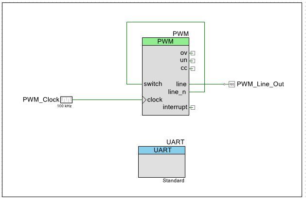
I have been trying to get a glitchless PWM working on a PSoC 4200 (I had in the past and was dusting off the old project), and I cannot seem to get the PWM Swap to work no matter what I try. I have attached a project that instantiates a PWM. I have the Line output connected to an LED so I can see the output of the PWM (it's on a CY8CKIT-049-42xx, so port 1.6), and am driving the PWM clock with a 1Hz clock so I can easily time the LED changing. In the configuration for the PWM component in PSoC Creator 4.3, I set the Period to 9 (I want a period of 10 seconds, and the datasheet says to set it to N - 1... that seems to work fine). I set the Compare Register to 2, I set the Compare Register Buffer to 6, and I turn on the Swap flag. The PWM is set to left align mode as well, and have turned off the interrupt. I'm keeping it simple with my example. The code in main does two things (my component is named PWM): "PWM_Start(); for(;;) CySysPmSleep();" ... so start the PWM component and put the processor to sleep. This is the simplest configuration I could come up with and it still doesn't work for me.
I program it into the 4200 and ... the LED stays on for 2 seconds, stays off for 8 seconds, stays on for 2 seconds, stays off for 8... etc. The Compare Register Buffer value never gets swapped with the Compare Register at TC per the documentation. I have tried a very large number of things including using the software to also set the swap flag to on ("PWM_SetCompareSwap(1);"), I've checked that the "ov" output is pulsing every 10 seconds (yup). In the component configuration, I have changed the Compare Register value to 4 and the Compare Register Buffer value to 8 just to make sure I'm programming the chip, and ... on for 4 seconds, off for 6 seconds, etc... never swapping in the buffered value. I've looked at all the documentation I could find. I've tried turning on the "switch" input and connecting it to the "ov" output (with a falling edge trigger). Nothing has worked. I set up an interrupt handler (not in the attached example) and verified that it was being called at TC... yup... I could write a value into Compare Register Buffer from the interrupt handler and ... it never gets swapped into the Compare Register, so no matter what I write, the PWM only reacts to the initial value of the Compare Register.
I have a running application on an identical PSoC 4200 that uses this technique, but compiled it with a much older version of PSoC Creator (probably something in the 3.x timeframe) and I just duplicated the code over for this project, and it definitely does not work anymore. Has something in PSoC Creator broken, has the component implementation in PSoC Creator changed, am I missing something very simple? I know it's not the hardware having changed, because it's the the same chips that used to work. What is particularly galling is that in the PWM component configuration window, it actually shows the expected waveform from the Line output, and it shows it high for 2 clocks, and then low for 8, then high for 6 clocks, and then low for 4. That does hint that something has gone wrong somewhere. I'm stumped. Any thoughts?
I got a response from a member of the community [MotooTanaka] on what they ended up doing to try to get it to work. It was WAY more effort than I could have possibly expected, and even then wasn't the direction I wanted to move toward (it required software, and I wanted a purely hardware solution if possible). Note: It's interesting in that it uses the serial port out to the PC as a status output, which is a good thing to remember that I can do when debugging (I forget sometimes).
Yes, this was(is) a very tough one. Just like you I tried for a few hours with series of failures... And in the datasheet of TCPWM, I found the following description:
This sounds like we need a "switch" event before the "TC" event. So I made the following project, using CY8CKIT-042. Note: Actually the following is the only project I could make the swap work. And in the ISR I needed to put CyDelay(2) to generate a long enough pulse width from the Control_Reg. Probably it could be done in the main loop. After that I tried a several hardware approaches but in vain. So my current conclusion is that we seem to need provide "switch" event before TC event, and it must have enough pulse width for PWM to detect (or set something inside).
( Schematic, pinouts, source code, and log output behind cut )
Again, I wanted a purely hardware solution, but... this laid the foundation for the solution. I wrote back:
I am overwhelmed by how much work you put into this. Thank you so much!
My frustration was that I definitely had it working, and it definitely was not working in this case. The documentation is quite contradictory, but your statement that a "switch" event is required matches my previous experience (and probably some random note I found somewhere when I was doing my earlier design). Your investigation and success doing it with an interrupt routine in software, led me to figure it out. Your statement that "I needed to put CyDelay(2) to generate a long enough pulse width" was what allowed me to find the relevant pieces of documentation that explained the situation.
The first piece of relevant information is at the bottom of the "Outputs" section of the TCPWM datasheet: "The overflow (ov), underflow (un), and compare/capture (cc) output signals have two HFCLK cycle pulse width for PSoC 4100/PSoC 4200 devices". So the "ov" output pulse is only two HFCLK clock cycles wide. The other needed piece of information is at the bottom of the "Inputs" section: "All inputs are double synchronized in the TCPWM. The synchronizer is run at HFCLK speed. After that (just for PSoC 4000, PSoC 4100, PSoC 4200, (Timer/Counter, PWM modes)), these signals are synchronized with the component clock." So... the "switch" input is sampled on the rising edge of the PWM "clock" signal, which in my case for this test is 1Hz. Since the "ov" is such a short pulse, it is long, long gone before it can be sampled by the 1Hz input clock if the "ov" signal is just looped back to the "switch" signal (which is what my original design that worked did). I should further mention to anyone reading this that the description of the Compare Swap feature in the datasheet is wrong. It currently says, "the swap selection causes the two compare values to swap at each TC event"; but it should say "the swap selection causes the two compare values to swap at each TC event if a switch event has occurred".
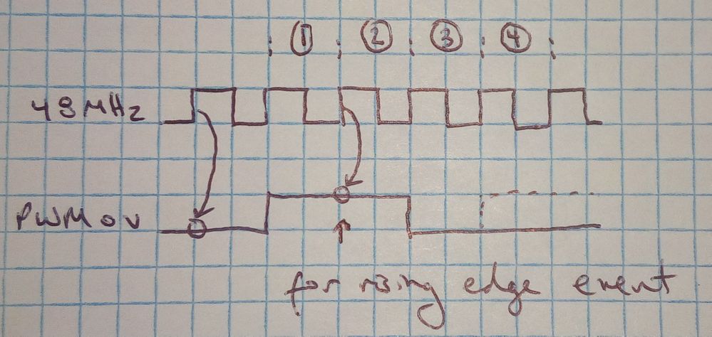
Then there's the question of why my earlier design did work. The answer to that makes sense now as well: I was clocking the PWM at HFCLK (48MHz in my case), so in looping the "ov" signal back to "switch" worked fine at triggering a switch event. The "ov" pulse is two HFCLK clock cycles long, and I had the "switch" configuration parameter set to trigger on a falling edge pulse, so the "switch" input would properly sample the high pulse because it was high long enough to be latched by the HFCLK clock signal, and then would properly sample the "ov" output going low again, and would trigger a switch event for the next TC. It would work as well if I had it set to switch on a low to rising edge. It seems I was just lucky with my earlier design because I didn't realize the "ov" signal issue -- I assumed it was clocked out with the PWM clock and would be high for one full PWM clock cycle (I was wrong on the number of clock cycles too since it is high for two HFCLK cycles) as this makes more sense to me as it allows for a full and easy hardware implementation of the register swapping at lower PWM clock frequencies. I think Cypress designers made a bit of a mistake with this decision to use an HFCLK-based pulse rather than a signal clocked with the PWM "clock" signal. Oh well, they're not going to be able to change it now as this is a hardware component and it can be made to work.
I really do want to do my design in hardware, so I figured out a way of using the on-chip programmable logic to allow the "ov" output to generate a signal usable by the "switch" input circuitry. This is an all-hardware solution as well. The Period has to be set to at least 2 (N - 1), so the PWM counts for at least 3 PWM clock cycles. The switch input is set to be a rising edge triggered event.The software is the same (turn on the PWM component and put the processor to sleep). Project attached.
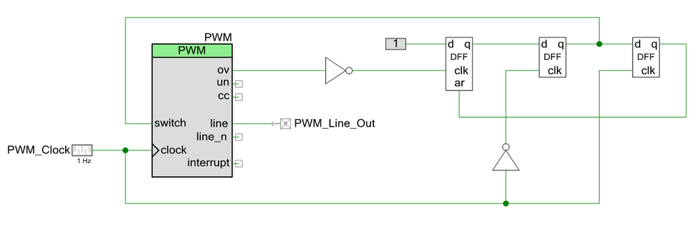
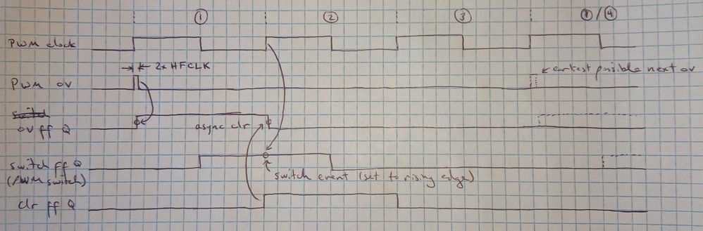
There is definitely a chance for metastability issues since we don't know precisely what the phase relationship is between the HFCLK and the PWM "clock". To that end, I invert the "ov" signal before clocking the first flip-flop with it. This guarantees at least two HFCLK cycles between when the PWM clock goes high (to trigger the "ov" signal) and when the "ov" signal goes low again at the end of the pulse. Depending on how the "ov" pulse is generated, it could be three or more HFCLK cycles before the falling edge (since it is a signal potentially going between clock domains, they probably have a synchronizer on it). As long as half the cycle time of the PWM clock is longer than the maximum time between the rising edge of the PWM clock and the falling edge of "ov" (plus the time needed for the signal to propagate through the first flip-flop to its Q output and the setup time needed for the second flip flop before it is clocked by the low-going edge of the PWM clock), then there will be no metastability problems. Because I'm not sure what the worst case is for when the "ov" pulse happens after the PWM clock triggers the signal (by causing the count to roll over from TC to 0), I can't make a guess at what the maximum safe frequency would be for this circuit. I'm sure it's fine into the MHz region, but I can't know for sure.
Here's the timing diagram for the above circuit:
Depending on the PWM clock frequency you need, if it's high enough and there's a worry about metastability, just clock the PWM at HFCLK and use the prescaler setting to bring the frequency down to where you need it. Since the prescaler can go from 1 to 128 (in powers of 2), use HFCLK/128 as the upper limit of where you might need to use this circuit. So for a 48MHz HFCLK, upper limit would be 375kHz (and for anything below that you probably need to use this circuit to get the switch swap to work). I have attached my modified circuit. Note that the project generates two warnings because PSoC Creator 4.3 recognizes that the circuit goes between clock domains without proper synchronization. As described above, the timing is okay as long as the PWM cycle time is sufficiently long compared to when the falling edge of "ov" occurs.
With these high and low speed techniques available for doing the Compare Register swapping, it can be done with any PWM clock frequency. Either allows for the glitchless operation of the PWM where the Compare Register Buffer can be updated in an interrupt handler triggered by the PWM TC event. The Buffered value is then automatically and cleanly swapped into the Compare Register at the TC event because a switch event happened in the last cycle. As long as the interrupt handler can run before the TC (in my earlier project, I used a Period count of 2177 at 48MHz, and woke the CPU up from a CySysPmSleep to process the interrupt, and there was plenty of time). The code I used in my old project to do this was as follows. I, of course, turned on the Interrupt on Terminal Count option on the PWM component and attached an Interrupt component (called "PWM_TC_ISR" in the code here).
Thank you again very much for your help!
To which the community member goes S-Tier and answers:
Thank you very much for your throughout explanation! Finally I understood with what we were fighting yesterday. BTW, reading your "paper", following (a kind of) stupid Idea came to my mind. At first I thought that I'd use a counter to generate the switch event. But we need to avoid immediate after the TC, and the width must be 2 or greater. Seeing the PWM configure dialog,
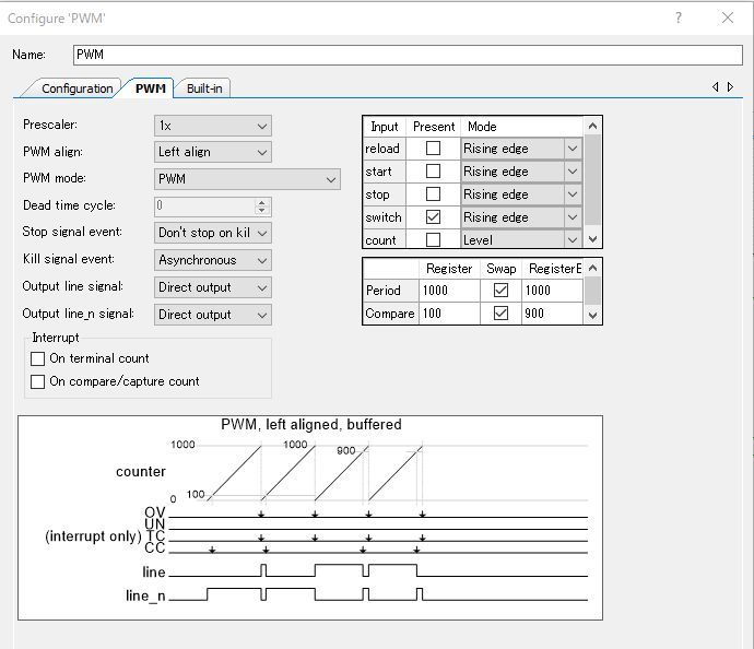
I thought... didn't we have a "counter" here? So if, and only IF, you can keep the compare between 2 to period-2, line_n seems to work for the purpose. So I modified the schematic as:
And... it works!
As I wrote above this trick works only 2 ~ period-2, but if your application put up with this limitation, this is quite an easy trick. Last but not least, I agree with you that the description in the datasheet was not kind nor sufficient for usual people like us.
Mind. Blown. So simple, so beautiful!
Hahahaha, I used a sledgehammer to solve the problem, and once the requirements were clear, you used a feather! That is definitely the optimal solution for the Compare register swap problem in almost all cases (provided, as you say, one can live within the compare value limitations), and it requires no additional system resources.
If you use a "Falling edge" trigger instead on the "switch" input, there is no limitation on the upper value for the Compare value (it can equal Period). Also, because the Period is actually set to N - 1 of the number of cycles (N) you want to count to [from the Period description for the PWM mode in the datasheet: "to cause the counter to count for N cycles, this register should be written with N-1 (counts from 0 to period inclusive)"], you can also go as low as 1 in the Compare register. I tested this with your loopback configuration and the Falling Edge trigger of "switch" with a Period of 9 (10 clock cycles), with a Compare Register of 1 and a Compare Register Buffer of 9, and it worked fine. I have attached the project.
Thank you again for providing a truly elegant solution to this problem.
And this, my friends, is how community can work together to solve hard to understand problems in elegant ways.
And here's more entertainment... Season 1, Episode 22:
I have been trying to get a glitchless PWM working on a PSoC 4200 (I had in the past and was dusting off the old project), and I cannot seem to get the PWM Swap to work no matter what I try. I have attached a project that instantiates a PWM. I have the Line output connected to an LED so I can see the output of the PWM (it's on a CY8CKIT-049-42xx, so port 1.6), and am driving the PWM clock with a 1Hz clock so I can easily time the LED changing. In the configuration for the PWM component in PSoC Creator 4.3, I set the Period to 9 (I want a period of 10 seconds, and the datasheet says to set it to N - 1... that seems to work fine). I set the Compare Register to 2, I set the Compare Register Buffer to 6, and I turn on the Swap flag. The PWM is set to left align mode as well, and have turned off the interrupt. I'm keeping it simple with my example. The code in main does two things (my component is named PWM): "PWM_Start(); for(;;) CySysPmSleep();" ... so start the PWM component and put the processor to sleep. This is the simplest configuration I could come up with and it still doesn't work for me.
I program it into the 4200 and ... the LED stays on for 2 seconds, stays off for 8 seconds, stays on for 2 seconds, stays off for 8... etc. The Compare Register Buffer value never gets swapped with the Compare Register at TC per the documentation. I have tried a very large number of things including using the software to also set the swap flag to on ("PWM_SetCompareSwap(1);"), I've checked that the "ov" output is pulsing every 10 seconds (yup). In the component configuration, I have changed the Compare Register value to 4 and the Compare Register Buffer value to 8 just to make sure I'm programming the chip, and ... on for 4 seconds, off for 6 seconds, etc... never swapping in the buffered value. I've looked at all the documentation I could find. I've tried turning on the "switch" input and connecting it to the "ov" output (with a falling edge trigger). Nothing has worked. I set up an interrupt handler (not in the attached example) and verified that it was being called at TC... yup... I could write a value into Compare Register Buffer from the interrupt handler and ... it never gets swapped into the Compare Register, so no matter what I write, the PWM only reacts to the initial value of the Compare Register.
I have a running application on an identical PSoC 4200 that uses this technique, but compiled it with a much older version of PSoC Creator (probably something in the 3.x timeframe) and I just duplicated the code over for this project, and it definitely does not work anymore. Has something in PSoC Creator broken, has the component implementation in PSoC Creator changed, am I missing something very simple? I know it's not the hardware having changed, because it's the the same chips that used to work. What is particularly galling is that in the PWM component configuration window, it actually shows the expected waveform from the Line output, and it shows it high for 2 clocks, and then low for 8, then high for 6 clocks, and then low for 4. That does hint that something has gone wrong somewhere. I'm stumped. Any thoughts?
I got a response from a member of the community [MotooTanaka] on what they ended up doing to try to get it to work. It was WAY more effort than I could have possibly expected, and even then wasn't the direction I wanted to move toward (it required software, and I wanted a purely hardware solution if possible). Note: It's interesting in that it uses the serial port out to the PC as a status output, which is a good thing to remember that I can do when debugging (I forget sometimes).
Yes, this was(is) a very tough one. Just like you I tried for a few hours with series of failures... And in the datasheet of TCPWM, I found the following description:
void TCPWM_SetCompareSwap(uint32 swapEnable)

Description:
Writes the register that controls whether the compare registers are swapped. When enabled in Timer/Counter mode (without capture) the swap occurs at a compare/capture event. In PWM mode the swap occurs at the next TC event following a hardware switch event. Not applicable for Timer/Counter with Capture or in Quadrature Decoder modes.

Parameters:
uint32 swapEnable: 0 = Disable swap; 1 = Enable swap.
This sounds like we need a "switch" event before the "TC" event. So I made the following project, using CY8CKIT-042. Note: Actually the following is the only project I could make the swap work. And in the ISR I needed to put CyDelay(2) to generate a long enough pulse width from the Control_Reg. Probably it could be done in the main loop. After that I tried a several hardware approaches but in vain. So my current conclusion is that we seem to need provide "switch" event before TC event, and it must have enough pulse width for PWM to detect (or set something inside).
( Schematic, pinouts, source code, and log output behind cut )
Again, I wanted a purely hardware solution, but... this laid the foundation for the solution. I wrote back:
I am overwhelmed by how much work you put into this. Thank you so much!
My frustration was that I definitely had it working, and it definitely was not working in this case. The documentation is quite contradictory, but your statement that a "switch" event is required matches my previous experience (and probably some random note I found somewhere when I was doing my earlier design). Your investigation and success doing it with an interrupt routine in software, led me to figure it out. Your statement that "I needed to put CyDelay(2) to generate a long enough pulse width" was what allowed me to find the relevant pieces of documentation that explained the situation.
The first piece of relevant information is at the bottom of the "Outputs" section of the TCPWM datasheet: "The overflow (ov), underflow (un), and compare/capture (cc) output signals have two HFCLK cycle pulse width for PSoC 4100/PSoC 4200 devices". So the "ov" output pulse is only two HFCLK clock cycles wide. The other needed piece of information is at the bottom of the "Inputs" section: "All inputs are double synchronized in the TCPWM. The synchronizer is run at HFCLK speed. After that (just for PSoC 4000, PSoC 4100, PSoC 4200, (Timer/Counter, PWM modes)), these signals are synchronized with the component clock." So... the "switch" input is sampled on the rising edge of the PWM "clock" signal, which in my case for this test is 1Hz. Since the "ov" is such a short pulse, it is long, long gone before it can be sampled by the 1Hz input clock if the "ov" signal is just looped back to the "switch" signal (which is what my original design that worked did). I should further mention to anyone reading this that the description of the Compare Swap feature in the datasheet is wrong. It currently says, "the swap selection causes the two compare values to swap at each TC event"; but it should say "the swap selection causes the two compare values to swap at each TC event if a switch event has occurred".
Then there's the question of why my earlier design did work. The answer to that makes sense now as well: I was clocking the PWM at HFCLK (48MHz in my case), so in looping the "ov" signal back to "switch" worked fine at triggering a switch event. The "ov" pulse is two HFCLK clock cycles long, and I had the "switch" configuration parameter set to trigger on a falling edge pulse, so the "switch" input would properly sample the high pulse because it was high long enough to be latched by the HFCLK clock signal, and then would properly sample the "ov" output going low again, and would trigger a switch event for the next TC. It would work as well if I had it set to switch on a low to rising edge. It seems I was just lucky with my earlier design because I didn't realize the "ov" signal issue -- I assumed it was clocked out with the PWM clock and would be high for one full PWM clock cycle (I was wrong on the number of clock cycles too since it is high for two HFCLK cycles) as this makes more sense to me as it allows for a full and easy hardware implementation of the register swapping at lower PWM clock frequencies. I think Cypress designers made a bit of a mistake with this decision to use an HFCLK-based pulse rather than a signal clocked with the PWM "clock" signal. Oh well, they're not going to be able to change it now as this is a hardware component and it can be made to work.
I really do want to do my design in hardware, so I figured out a way of using the on-chip programmable logic to allow the "ov" output to generate a signal usable by the "switch" input circuitry. This is an all-hardware solution as well. The Period has to be set to at least 2 (N - 1), so the PWM counts for at least 3 PWM clock cycles. The switch input is set to be a rising edge triggered event.The software is the same (turn on the PWM component and put the processor to sleep). Project attached.
There is definitely a chance for metastability issues since we don't know precisely what the phase relationship is between the HFCLK and the PWM "clock". To that end, I invert the "ov" signal before clocking the first flip-flop with it. This guarantees at least two HFCLK cycles between when the PWM clock goes high (to trigger the "ov" signal) and when the "ov" signal goes low again at the end of the pulse. Depending on how the "ov" pulse is generated, it could be three or more HFCLK cycles before the falling edge (since it is a signal potentially going between clock domains, they probably have a synchronizer on it). As long as half the cycle time of the PWM clock is longer than the maximum time between the rising edge of the PWM clock and the falling edge of "ov" (plus the time needed for the signal to propagate through the first flip-flop to its Q output and the setup time needed for the second flip flop before it is clocked by the low-going edge of the PWM clock), then there will be no metastability problems. Because I'm not sure what the worst case is for when the "ov" pulse happens after the PWM clock triggers the signal (by causing the count to roll over from TC to 0), I can't make a guess at what the maximum safe frequency would be for this circuit. I'm sure it's fine into the MHz region, but I can't know for sure.
Here's the timing diagram for the above circuit:
Depending on the PWM clock frequency you need, if it's high enough and there's a worry about metastability, just clock the PWM at HFCLK and use the prescaler setting to bring the frequency down to where you need it. Since the prescaler can go from 1 to 128 (in powers of 2), use HFCLK/128 as the upper limit of where you might need to use this circuit. So for a 48MHz HFCLK, upper limit would be 375kHz (and for anything below that you probably need to use this circuit to get the switch swap to work). I have attached my modified circuit. Note that the project generates two warnings because PSoC Creator 4.3 recognizes that the circuit goes between clock domains without proper synchronization. As described above, the timing is okay as long as the PWM cycle time is sufficiently long compared to when the falling edge of "ov" occurs.
With these high and low speed techniques available for doing the Compare Register swapping, it can be done with any PWM clock frequency. Either allows for the glitchless operation of the PWM where the Compare Register Buffer can be updated in an interrupt handler triggered by the PWM TC event. The Buffered value is then automatically and cleanly swapped into the Compare Register at the TC event because a switch event happened in the last cycle. As long as the interrupt handler can run before the TC (in my earlier project, I used a Period count of 2177 at 48MHz, and woke the CPU up from a CySysPmSleep to process the interrupt, and there was plenty of time). The code I used in my old project to do this was as follows. I, of course, turned on the Interrupt on Terminal Count option on the PWM component and attached an Interrupt component (called "PWM_TC_ISR" in the code here).
CY_ISR(PWM_Next_Value) {
    PWM_WriteCompareBuf(<>);
    PWM_ClearInterrupt(PWM_INTR_MASK_TC); }

int main() {
    PWM_TC_ISR_StartEx(PWM_Next_Value); PWM_Init();

    // Write the first two samples into the PWM
    PWM_WriteCompare(<>);
    PWM_WriteCompareBuf(<>);

    CyGlobalIntEnable; PWM_Enable();  // Only starts it, does not re-initialize
    for(;;) { CySysPmSleep(); } }
Thank you again very much for your help!
To which the community member goes S-Tier and answers:
Thank you very much for your throughout explanation! Finally I understood with what we were fighting yesterday. BTW, reading your "paper", following (a kind of) stupid Idea came to my mind. At first I thought that I'd use a counter to generate the switch event. But we need to avoid immediate after the TC, and the width must be 2 or greater. Seeing the PWM configure dialog,
I thought... didn't we have a "counter" here? So if, and only IF, you can keep the compare between 2 to period-2, line_n seems to work for the purpose. So I modified the schematic as:
And... it works!
As I wrote above this trick works only 2 ~ period-2, but if your application put up with this limitation, this is quite an easy trick. Last but not least, I agree with you that the description in the datasheet was not kind nor sufficient for usual people like us.
Mind. Blown. So simple, so beautiful!
Hahahaha, I used a sledgehammer to solve the problem, and once the requirements were clear, you used a feather! That is definitely the optimal solution for the Compare register swap problem in almost all cases (provided, as you say, one can live within the compare value limitations), and it requires no additional system resources.
If you use a "Falling edge" trigger instead on the "switch" input, there is no limitation on the upper value for the Compare value (it can equal Period). Also, because the Period is actually set to N - 1 of the number of cycles (N) you want to count to [from the Period description for the PWM mode in the datasheet: "to cause the counter to count for N cycles, this register should be written with N-1 (counts from 0 to period inclusive)"], you can also go as low as 1 in the Compare register. I tested this with your loopback configuration and the Falling Edge trigger of "switch" with a Period of 9 (10 clock cycles), with a Compare Register of 1 and a Compare Register Buffer of 9, and it worked fine. I have attached the project.
Thank you again for providing a truly elegant solution to this problem.
And this, my friends, is how community can work together to solve hard to understand problems in elegant ways.
And here's more entertainment... Season 1, Episode 22:


